
How Much Does a High-Density PCB Cost?
High-Density PCB Cost
HDI is a high density interconnect technology that allows PCBs to pack more components into a smaller space. It improves signal integrity by reducing the distance between components. As a result, it is possible to reduce the size of gadgets while maintaining their functionality and performance.
Using high density interconnect pcb requires careful consideration of design and manufacturing techniques to avoid problems. It’s important to choose a manufacturer with experience in working with HDI. They should have the equipment and technical expertise to ensure that your project is a success.
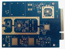
The amount that a high-density PCB costs depends on the type of manufacturing technique and the number of layers used. The more layers you need, the higher the price will be. The choice of vias, through-holes or microvias will also impact the cost. Smaller vias require more precision and can be more expensive than larger ones.
How Much Does a High-Density PCB Cost?
When designing for HDI, it’s important to consider how the various manufacturing methods affect the resulting cost and quality of the final product. In order to avoid issues, the design team should select the best material for use with the desired fabrication process. Several factors should be taken into account, including the coefficient of thermal expansion (CTE), resistance to stress, and dielectric constant. Additionally, it is essential to design a circuit board with adequate layer counts and trace widths, while avoiding over-drilling.
One of the most challenging aspects of designing for HDI is ensuring that the board’s layout is suitable for its intended manufacturing process. This includes determining the maximum ball pitch for BGA components, and ensuring that the layout meets the required via sizes. It’s also important to choose the correct copper materials, and consider their CTE values, temperature ratings, and electrical characteristics. The selection of the right materials is critical because it will influence the reliability and performance of the finished product.
The layout of an HDI PCB is typically more complex than that of a traditional printed circuit board, which can cause problems when it comes to production. This is because the layout requires a more rigorous metallization process. The resulting complexity can also make it difficult to place the component leads correctly. Fortunately, there are a number of tools available to help reduce the risk of errors during the layout process.
Choosing the correct copper plating method is also crucial for HDI boards. This is because it has a direct impact on the thickness of the copper and the overall finish. In addition, the etch rate should be controlled to prevent over-etching and to preserve the isolation line.
Another challenge of manufacturing an HDI PCB is the drill-to-copper clearance, which is defined as the distance between the edge of a drilled hole and the nearest copper feature. This clearance can be improved by implementing a landless via technology, which is a laser-based method of drilling that eliminates the need for pads. It also reduces the size of the PCB by up to 20%.

Maine secretary of state disqualifies Trump from primary ballot

Trump to hold D.C. rally on Jan. 19, the day before his inauguration

18 states sue Trump administration over order seeking to overturn birthright citizenship
About The Author
