
What are the types of vias used in HDI PCB?
HDI PCB
In high density interconnect (HDI) PCBs, the vias play a vital role in signal transmission. The size and depth of the vias and the length of the traces are crucial to achieving optimal performance of high-speed signals. Vias are copper-plated holes or cylinders that connect the inner layers of the board to each other. They may be visible from the top or bottom of the board or they can be hidden in the layers. The latter are called blind vias because they do not pass through the entire circuit board and are only visible from one side. Blind vias must be 6 mils and less in diameter to ensure proper connectivity between layers.
During the manufacturing process, copper plating is used to fill the drilled holes with metal to complete the electrical connection. Conductive plating improves current flow between layers and reduces heat generation caused by large components like ICs and BGAs. There are two primary methods of copper plating: electroless and electrolytic. Both methods are important for the success of HDI manufacturing because they provide the necessary thickness to ensure conductive integrity between layers.
The choice of a particular stack-up is also critical to the successful manufacture of an hdi pcb. The number of layers and the material type directly impact manufacturing costs. There are several different types of stack-ups that can be used to achieve the desired level of functionality, cost, and quality.
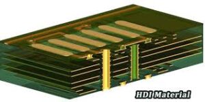
What are the types of vias used in HDI PCB?
A typical HDI structure has multiple levels of microvias that connect to the underlying layers. Each level has a specific purpose and a specific method of assembly. These vias can be either stacked or staggered. Staggered vias are drilled in different layers and piled on top of each other, while stacked vias are arranged in a pattern that is layered in between the other microvias.
Depending on the layer count of an HDI circuit board, the structure may also include buried vias. These are not etched but are filled with low CTE epoxy resins and then capped with copper. This type of construction is commonly used to assemble BGAs and Surface Mount Devices (SMDs) onto the same drilled pads. Another type of via used in an HDI PCB is a near-pad via. These are smaller than standard through-hole vias and are designed to be used as a substitute for a solder joint. The advantage of this design is that it eliminates the need for solder joints and reduces overall manufacturing time.
The type of via used in an HDI circuit board can have a direct effect on its reliability. For example, a through-hole via that is not plated will have a higher chance of failing due to drill wander and other factors. In contrast, a near-pad via is more reliable because it will have more surface area and can be easily re-routed in the event of failure.

What Will Be the Song of the Summer?
What Design Tools Are Used For Printed Circuit Board Prototypes?

The Hater’s Lament
About The Author
